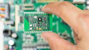
Used in Assembling Circuit Boards
The assembly of a circuit board is a complex process and can involve many different steps. It’s important to follow best PCBA practices in order to ensure that the SMT process goes smoothly and the final product is of high quality.
Surface mount technology (SMT) eliminates the need for drilled holes and manual insertion by mounting components directly onto a printed circuit board’s surface. This allows for much smaller devices to be made with the same functionality and performance of traditional through-hole components.
SMT is also more efficient than traditional through-hole manufacturing methods because it can be automated using pick and place machines. This reduces human error and speeds up the production time.
These machines can place components on a assembled circuit board accurately according to the designs that have been laid out by the designer. This makes SMT a more cost-effective and accurate way to produce electronic devices.
Typically, SMT components have smaller leads than their through-hole counterparts, or they don’t have any at all. This means that they can be placed in the same location on a circuit board as through-hole components, but with much higher densities. It also allows for more components to be mounted on a single side of the circuit board, which can improve the efficiency and reliability of the device.
How SMT Can Be Used in Assembling Circuit Boards
A key factor in a successful SMT assembly is proper soldering. This is done by using a solder paste that has been screened through a metal stencil onto the circuit board’s copper pads. The paste should have a tin, gold, nickel/gold or palladium coating that inhibits oxidation. In addition, it must contain a flux and a solder material such as tin, lead, or an organic solderability preserver.
Once the solder paste has been applied to the pads, it is melted by the SMT machine. The melted solder is then applied to the components, which are then carefully positioned on the circuit board by hand or by a robot. The machines can apply a precise amount of solder to each component, which is crucial for correct operation and signal transmission.
After the solder has cooled, it is inspected one last time by a 3D automated optical inspection machine to make sure that there are no defects in the soldering or incorrect placement of components. The AOI machine can also check that the solder has fully bonded to the components.
Once the circuit board has been inspected, it is ready for assembly and manufacturing. It can then be connected to other electronic components and a protective housing. The finished circuit board is now a complete, functioning device that can be shipped to customers around the world. This process is a significant step forward in the production of electronic devices, and it offers a wide range of benefits for consumers and manufacturers alike. It is also environmentally friendly, as fewer materials are used and waste is reduced. This method of manufacturing is expected to continue to grow in popularity as the demand for electronics continues to increase.