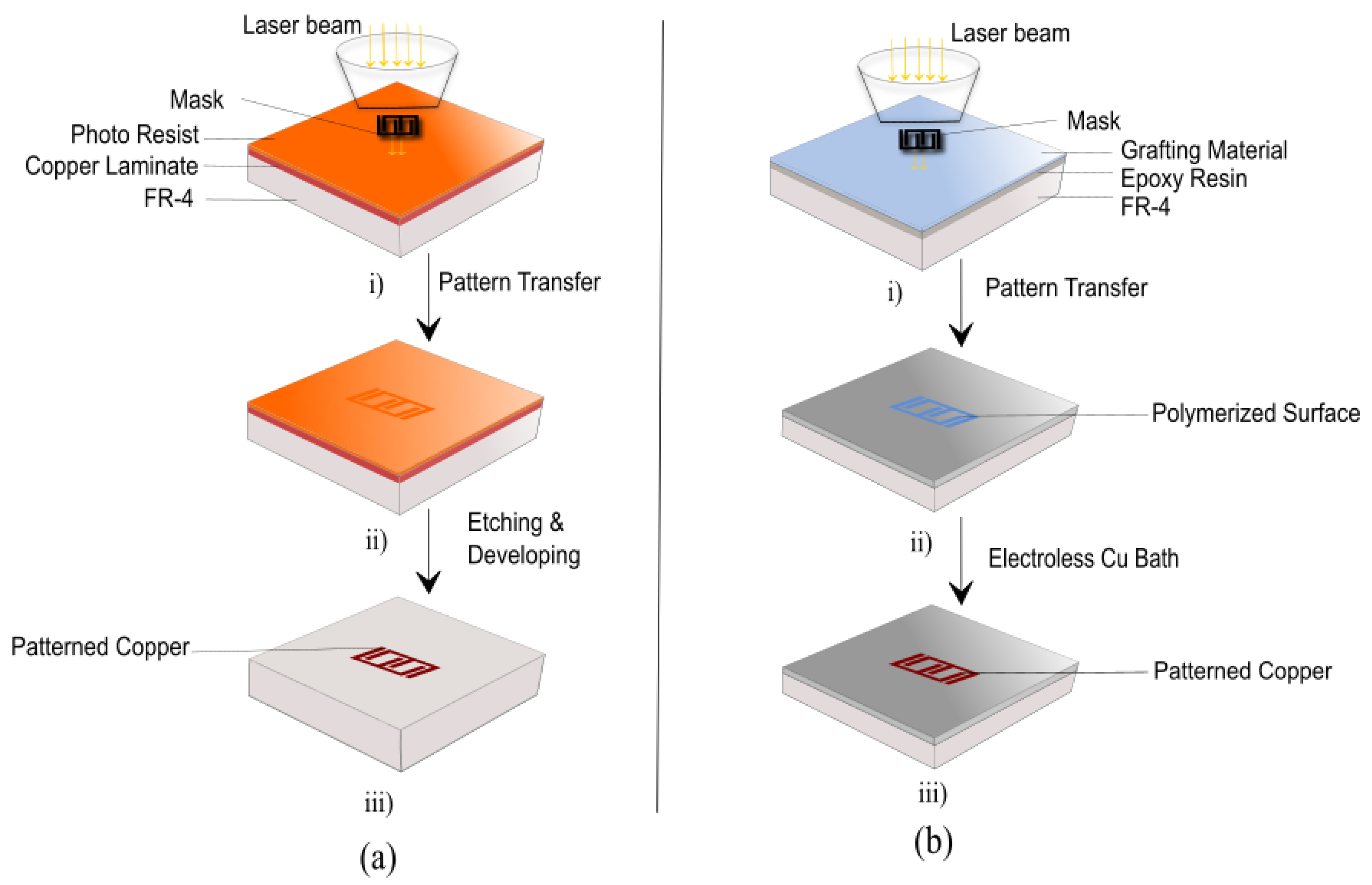
RF PCB Fabrication
There are many different RF PCB fabrication techniques, such as etching and laser direct imaging. These processes can help to maintain a high-quality board, with minimal deviation in the through holes (PTHs). These are important for maintaining impedance matching and minimising signal reflection and noise. RF PCBs also require careful placement of components and transmission lines to minimize parasitic capacitance and inductance.
Choosing the right materials for RF circuit boards is essential for proper operation. This includes selecting a substrate material with the right loss characteristics at RF frequencies. Suitable materials include polytetrafluoroethylene, ceramics, hydrocarbons, and different forms of glass. Rogers material is a common choice for rf pcb due to its low loss characteristics and dielectric constant.
The RF PCB stack-up should be designed to isolate the traces and components from each other, which helps to ensure signal integrity. This is achieved by placing the RF copper traces and components on the top layer, followed by a ground plane, power supply, and non-RF components. This provides a controlled return path for the signals, reducing crosstalk and improving overall performance.
RF PCB Fabrication Techniques
Impedance matching is essential for RF PCB design, as it can significantly reduce signal loss and improve the circuit’s performance. In addition to matching the characteristic impedance of the transmission line, it is also necessary to consider factors like the length and width of the trace, the thickness of the layer, and the type of dielectric used. The RF PCB’s transmission line structure must also be carefully chosen, with the most appropriate structures being microstrips, striplines, or coplanar waveguides.
It is important to minimize the length of RF transmission lines, as long traces can increase signal losses. This can be done by using isolation techniques and careful component placement, as well as by minimizing the number of layers and transmission lines.
Another important consideration is the use of decoupling capacitors, which are a vital part of any RF PCB. These capacitors help to remove the effects of interference, noise, and EMI. The capacitors should be placed on the component layer, connected in parallel to the RF chip’s Vcc and ground. In addition, it is important to choose the right capacitance value for these capacitors. For example, a 90-degree bend in a transmission line can add capacitance and change the characteristic impedance of the line.
Inductance can be minimized by ensuring that the ground plane is close to the RF signals and by ensuring that each RF signal has its own ground via. It is also crucial to make sure that the grounding connections are matched to the circuit’s characteristic impedance. The PCB’s design should also ensure that the grounding is stable and that there are no loops. Finally, it is important to ensure that the RF PCB can withstand vibrations and temperature fluctuations. This is achieved by using adequate thermal vias and heat sinks.