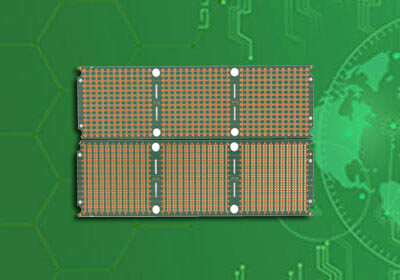
High Density Interconnect
Modern electronic devices packed with a wide range of capabilities are astoundingly compact. For example, a smartphone packs communication, computing, navigating, photography and various sensors in a small package that fits easily in the palm of your hand. This remarkable miniaturization is made possible by the use of high-density interconnect (HDI) printed circuit boards. HDI PCBs feature smaller traces and spacing widths than traditional PCBs, allowing for more components to be placed in the same space.
But despite the impressively small footprint of these devices, a high-density PCB requires a more intricate layer stackup configuration than a standard board. A key factor is the use of microvias, which allow for more connectivity between layers and a higher wiring density. A well-conceived design with a thorough understanding of the underlying PCB layer stackup will minimize impedance control routing calculations and ensure performance, thermal and signal integrity.
The process for making a multi-layer high density interconnect PCB starts with photoresist deposition and exposure to define the areas to be etched. This is followed by etching with the current industry standard etchant—a ferric chloride solution. Once the etching is complete, the remaining photoresist can be removed and the copper layer can be metallized. The result is a conductive pattern on the laminate, which is then ready for outer layer processing.
What is High Density Interconnect?
Another aspect of a multi-layer HDI PCB is the use of blind vias. These are holes drilled into the internal layers of the PCB and are only accessible from the top or bottom side of the board. These holes are not visible from the outside of the PCB and can only be accessed through a mechanical drill or laser. Once a blind via has been drilled, it can be filled with copper to provide a path for transferring signals between the top and bottom sides of the PCB.
Buried Vias are the opposite of blind vias, connecting two internal layers of an HDI PCB through a hole that is not visible on the surface of the board. These vias are drilled from the inside of the PCB and are plugged with an electroplated metal ball. Using these connections, the conductors on each side of the PCB can be connected freely.
The technology behind high-density interconnect PCBs is essential for the development of mobile phones, ultra-mobile computers and digital products. It is also employed in a wide variety of other digital and industrial electronics, including automotive electronics, IC carrier boards, and medical and military equipment. In all these cases, the smaller size and greater component density of an HDI PCB can help to reduce power consumption, enhance performance, and increase reliability. Whether your application requires a small footprint device or needs to handle high-speed data transmission, contact an experienced HDI PCB manufacturer to explore the possibilities of this innovative technology. You will be surprised at what is possible with this revolutionary innovation in PCB design.